Project Description
Summary
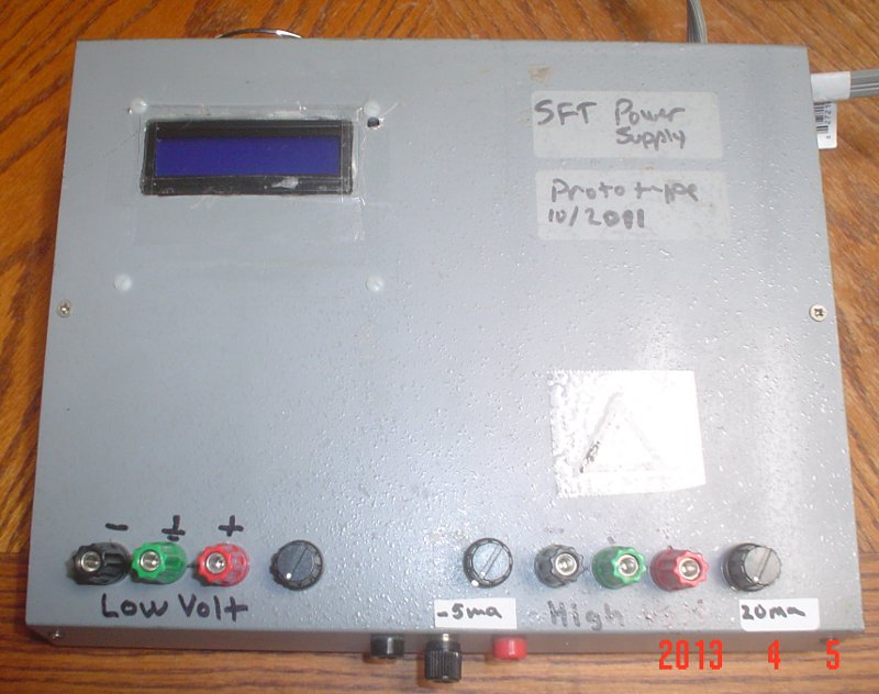
The SFT Power Supply is a switching power supply prototype that tests a number of 'Proof of Concept'
ideas regarding the use of an AVR microcontroller, some of which may be patentable. The basic design
uses the PWM outputs and analog inputs that are built into the AVR microcontroller to monitor a number
of parameters. The voltage is controlled using 0-5V output from 4 wirewound potentiometers on the front
panel next to the banana jacks. The left-most potentiometer controls the +/- 0 to 12V output setting,
and the right 2 potentiometers control the voltage on the nearby banana jack (-15 to -75V, 36 to 400V).
Why is this an 'Amazing Thing'?
Switching power supplies are often controlled by specialty electronic circuits that are typically
designed to control external devices as boost, buck, or boost-buck converters and voltage regulators.
In many cases, these specialty circuits actually cost MORE than a microcontroller. Additionally, since
a microcontroller can be programmed to perform many different tasks, a switching power supply can
become only one of many functions provided by the CPU.
The prototype bench power supply provides 3 regulated outputs using a single CPU. Two of these use
'charge pump' voltage multipliers to obtain high voltages. This could also be done using flyback, as
needed. The other two voltages have a matched +/- low voltage output, and are controlled using PWM.
Principles of Operation
The low voltage output uses 2 simple direct coupled transistor circuits to convert the 0-5V PWM output
of the AVR to an appropriate high current PWM output, into a 100uH load coil and a pair of filter
capacitors. Each output has a separate PWM signal controlling it. The AVR microcontroller's internal
timers are operated at much higher than normal frequencies to obtain better results with smaller
components.
The high voltage outputs are driven by an internal 'charge pump' voltage converter, consisting of a similar
direct-coupled transistor circuit with a 0-5V PWM input, to create an internal +45V 1A power supply. When
coupled with the -15V power supply another direct-coupled transistor circuit can generate an approximately
60VDC p-p PWM signal that drives the voltage multiplier for the 36V to 400V output. The minimum of 36V is
coincidental to voltage drop across the multiplier circuit (9 diodes in series). A similar voltage multiplier
circuit drives the -HV (-15 to -75V) output (using less expensive components).
The prototype internally has a simple +/-15V @2A unregulated power supply using a split-phase 120/24VCT
transformer, and the output from the unregulated power supply is available via jacks on the front panel.
These output jacks were intended for use by the calibration process but could still be used to provide power.
The true 'secret sauce' of the design involves the manner in which the software controls the voltages. Although
nothing is really all that complicated as far as the hardware is concerned, the software algorithm is a completely
different story. In short, it simulates a hardware device with predictive capability and alters the PWM output as
necessary to control the voltages. Many different voltage parameters, including the unregulated power supply
voltage and current, are measured and acted upon by the code in a continuous loop. The LCD display continuously
displays the 4 measured output voltages, temporarily switching to a different mode that displays the appropriate
voltage setting while you rotate one of the setting potentiometers. If an overcurrent condition is detected,
the PWM output is shut down, placing the unit in a safe condition (indicated by the LCD display). The 'overload'
condition can be reset by power-cycling the device.
Because of all of the internal measurements, and the use of NON-precision resistors and components (for lower cost),
a calibration process is needed. When performed manually, it takes a few minutes, using a command-line utility
and an RS232 adaptor (an RS232 connector is mounted on the side of the device for this purpose). The calibration
utility has you take specific measurements and record the voltmeter readings. Then it makes some calculations and
saves the calibration data into the AVR microcontroller's NVRAM.
Because the power supply is controlled by a microcontroller, MANY application possibilities exist. Several weeks
of careful research and design went into the firmware, as well as my own experience in control systems. Without
going into a lot of detail as to how I envision its use, there are several kinds of circuits in which a variable
voltage or current monitoring capability would come in handy. (I already have a lot of good application ideas, but
I'd really rather not mention any of them until I have working protoypes). But as a 'test bench' power supply for
electronics research, it already has a lot of value to me.
Features
- 4 regulated outputs: +/- 0 to 12V, -15 to -75V, 36 to 400V
- 2 unregulated outputs on front panel, +/- 15V
- All 4 regulated voltages displayed on LCD
- built-in short-circuit detection shuts down switcher output
- Low voltage outputs up to 2A
- Negative high voltage up to 5ma
- High voltage up to 20ma
- All output voltages created from +/- 15V @2A (unregulated)
- Calibration procedure via external software and serial port
- POSIX-compliant command line utility
- Also builds and runs on Microsoft Windows
- Procedure involves taking specific voltage measurements and recording the values
- Calibration data is stored to NVRAM on the AVR microcontroller
- Designed internally to be modular, with minimal hardware cost
- Designed with electrical safety in mind, with 2 internal fuses and a grounded power cord.
- One fuse is on the 'hot' side of the power cord, so that if it blows, no line voltage will be applied to any component
- Another fuse is on the internal 45V power supply to protect the HV power supply components from overload
(Early attempts had a tendency to fry the output transistors until I changed them out for higher rated components,
and the fuse protected the 45V power supply from being taken down along with the shorted-out transistors)
- Built-in cooling fan (mounted on the back, adapted from a Pentium CPU cooler) and steel case.
Project Status
- Initial prototype completed 10/2011
- recently modified 3/2013 to test the use of 4.7uF ceramic capacitors in the HV multiplier (improvement observed)
- Additional software work needed to improve low current voltage stability (it has a tendency to 'wiggle'
a bit in the 'less than 1% of scale' range). When the limits of the 10-bit A:D and 8-bit PWM are weighed
against a desired for a voltage accuracy of better than 0.1%, there are a few challenges to writing the
algorithm in a way that works around these limitations effectively.
- HV multiplier needs larger capacitors on the first 5 stages (or different power components) to improve current capacity
- PWM frequency is currently limited to 8khz due to switching crossover delay on output transistors
If the frequency is too high, the transistors overheat and are eventually destroyed.
- Lower frequencies require larger capacitors, in this case 100uF on the first stage
Larger valued electrolytic capacitors would be a safer alternative anyway, as they would also have higher ripple current and lower ESR
- The existing prototype uses 4.7uF ceramic capacitors on all HV multiplier stages, with electrolytic capacitors in
parallel with the first 4 stages.
- Using 100uF capacitors on the first stage, with decreasing values on the next 4 stages, should bring
the maximum current up to about 100ma @350V. Since the internal 45V power supply (which drives the
HV multiplier) is capable of delivering this kind of power, there is no real reason why it would not
work as expected.
- Capacitor choice is key, specifically with respect to the the maximum ripple current and ESR for
electrolytic capacitors; otherwise their life will be shortened and they may explode from overheating
- Even with the cost of the electrolytic capacitors and ceramic capacitors in the HV multiplier circuits, the cost
of the entire power supply would be significantly lower than that of a traditional iron transformer that would
likely be used to generate power supply voltages in excess of 300V, with additional benefits in weight reduction
and stray electro-magnetic coupling of the line frequency.
- Additional engineering work for the following
- Possible adaptation of the design for single-phase DC input of 16-24V, such as from a laptop power supply or battery
- Standard laptop computer switching power supplies are extremely inexpensive, and available pretty much everywhere at low cost,
and already contain line filtering and overcurrent protection circuits as well as FCC, CE, UL, and other 'approval' ratings
- One of the PWM outputs has already been reserved for the purpose of implementing an internal unregulated negative 'charge pump' power supply off of the positive supply
- Possible use of standard 'H bridge' or MOSFET (rather than complementary bipolar devices) for the high current PWM drivers
- Bipolar devices are less expensive but tend to overheat a bit more, and require additional circuitry to drive them with sufficient current
- enhancement MOSFET devices are more expensive, but have very low drive current requirements. However, an extra 'inverter' signal may be needed
to deal with crossover issues
- Existing 'H' bridge and 'half-H' bridge components may be too expensive for practical consideration, though they would greatly simplify the design
- MOSFET devices usually have much better high frequency and current handling characteristics for VERY HIGH CURRENT applications
- Board designs and FCC regulatory testing
- Appropriate faraday cage design for use as a general purpose power supply
Need reliable+indexpensive component source for inductors, as well as line filters and switching isolation transformers [for a possible
switching front-end]
Additional Photos
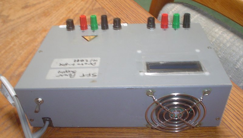
Back view of the prototype, showing the cooling fan
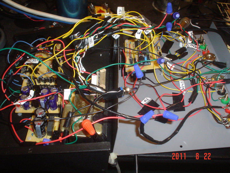
A view of the inside - multiple proto-boards and lots of wires!
|